

Chip Design
(4.9 Reviews)
Starting On : _____
VLSI Design Flow(EICT Academy-phase-II Scheme)
Course Description
The Training in Program on VLSI Design flow (Online Mode) aims to provide a comprehensive overview of Very Large Scale Integration concepts, covering digital design methodologies, RTL ,synthesis , physical design. Participants will gain hands-on experience with open source EDA tool , explore power-efficient design strategies, and delve into emerging trends. The course emphasizes practical applications through project work and offers insights from industry experts who have delivered 30+ chip tapeouts for top design houses like Intel, STMicroelectronics, NXP to name a few, enabling a foundational understanding of VLSI principles and practices in a condensed timeframe.
Prerequisites:-
- Basic knowledge of digital circuits and logic gates.
- Familiarity with a Unix/Linux environment and command-line interface
What you'll learn in this course?
- Overview of VLSI Design Flow
- Basics of Digital Electronics
- Linux Basics for VLSI Design
- Hardware Modeling with Verilog
- RTL Synthesis
- Physical Design (Floorplanning, Clock Tree Synthesis, Routing)
- Daily Course Breakdown
Duration & Timing
Program Length: 8 working days (42 Hours)
Total Training Hours: Over 42 hours of comprehensive learning and hands-on experience.
VLSI Design Training Schedule
| Day | Session 1 | Session 2 |
|---|---|---|
| Day 1 | Introduction to VLSI Design & Digital Electronics | Fundamentals of Digital Electronics (Logic Gates) |
| Day 2 | Combinational and Sequential Circuits | Hands-on: Simulating Logic Gates using Logisim/Deed Simulator |
| Day 3 | Linux Basics for VLSI Design | Hands-on: Linux Commands and VI Editor |
| Day 4 | Introduction to Verilog Programming | Hands-on: Verilog for Combinational Circuits |
| Day 5 | Verilog Programming | Hands-on: Simulation of Sequential Circuits in Verilog |
| Day 6 | Introduction to Synthesis | Hands-on: Synthesis with Yosys |
| Day 7 | Introduction to Physical Design | Hands-on: Physical Design Tools (OpenROAD/Qflow) |
| Day 8 | Review and Q&A | Online Feedback, Evaluation & Conclusion Session |
Eligibility Criteria
- Educational Qualifications:
- Polytechnic Staff, ITI Staff, Post-Graduate STEM Teachers, Research Scholars, Faculty, and Industry Professionals
Steps to Apply for the Course
- Yosys
- Magic
- iVerilog
- OpenSTA/ OpenTimer

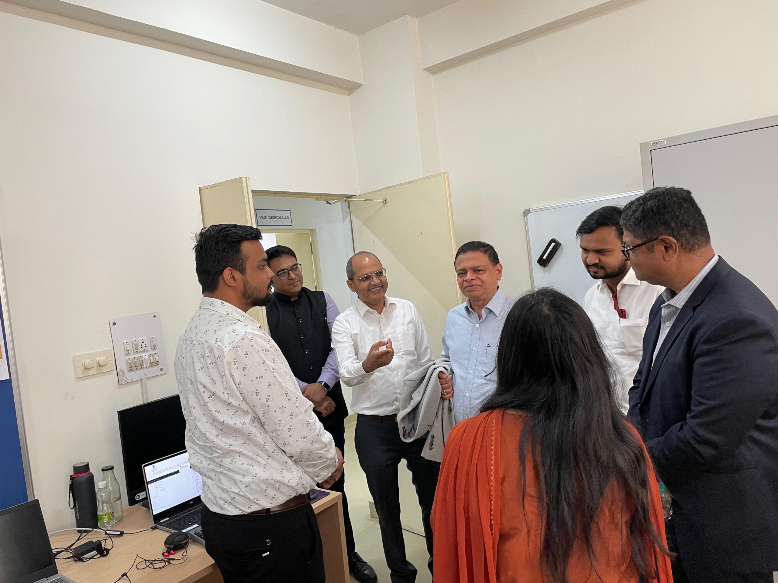
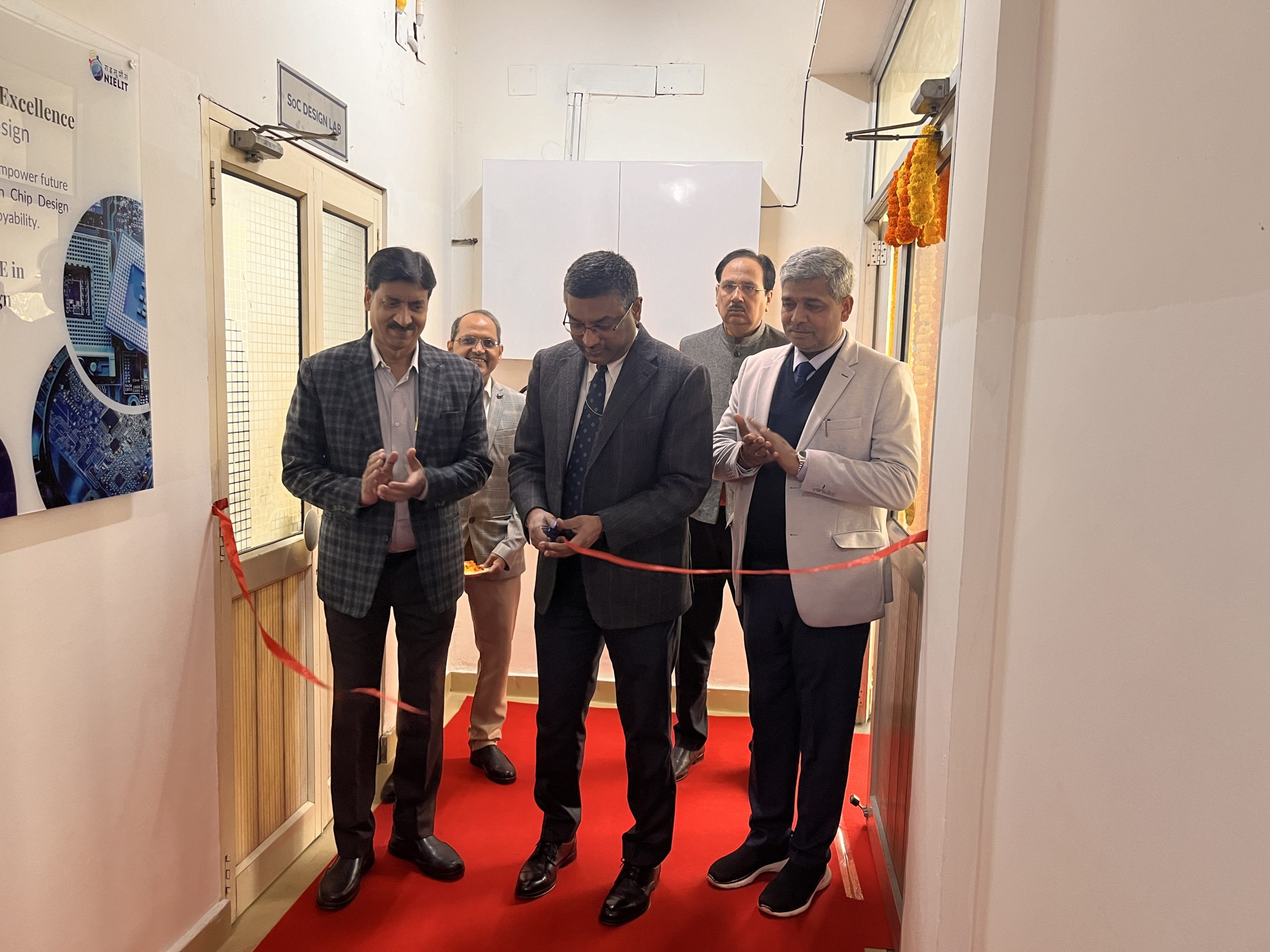
CoE in Chip Design, NIELIT Noida
Mr. Prashant Pal is a seasoned expert in the field of chip design with extensive experience in both academia and industry. As the Deputy Director and Scientist C at NIELIT Noida’s Centre of Excellence in Chip Design, he plays a pivotal role in advancing research and development in semiconductor technologies. With a deep understanding of VLSI design, he has successfully guided numerous projects and contributed to the development of cutting-edge solutions. His expertise and passion for chip design make him a highly respected mentor and instructor.

Course Fee:
No Fee
Course Includes:
- Level Intermediate
- Duration 42hr
- Sessions 16
- Mode Online
- Certification Yes
Frequently Asked Questions
Have questions? Find quick and clear answers to the most common queries in our FAQ section. Whether it’s about our programs, services, or initiatives, we’re here to provide the information you need to stay informed.”
Yes, we offer a 10% group discount for a minimum of 5 students or working professionals from the same university, institute, or company.
The Certification Programme in VLSI Design Flow incorporates industry-leading tools and resources to provide practical training in ASIC design workflows.
Genus: For logic synthesis and RTL design optimization.
Innovus: For physical design tasks like floor planning, placement, routing, and clock tree synthesis.
Tempus: For static timing analysis and timing closure.
Yes, we offer a two-part installment option for the course fees. For more details, please refer to the registration page.